


Sony takes us on a tour of its CMOS sensor design facility in Osaka
Jun 3, 2021
John Aldred
John Aldred is a photographer with over 25 years of experience in the portrait and commercial worlds. He is based in Scotland and has been an early adopter – and occasional beta tester – of almost every digital imaging technology in that time. As well as his creative visual work, John uses 3D printing, electronics and programming to create his own photography and filmmaking tools and consults for a number of brands across the industry.
Share:
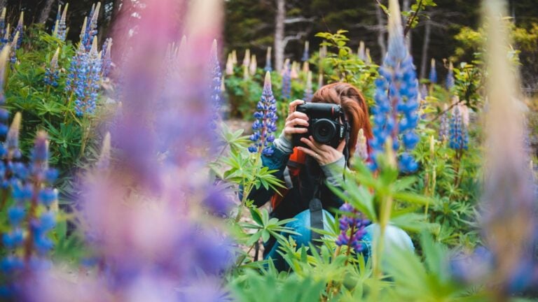
Tours of factories and facilities are always quite popular to see. We’ve seen quite a few over the years, too covering things like lens and camera construction. Occasionally it’s photography and filmmaking accessories and sometimes even making film. Sometimes, though, as is the case here, we get to see the philosophy of the facility itself.
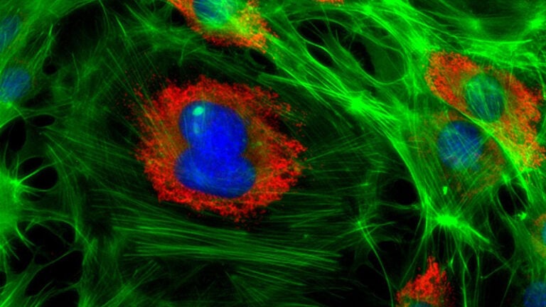
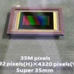
Sony has posted up a peek inside its Osaka Office. It’s a facility dedicated to CMOS sensor development and was designed by the engineers who work there in order to maximise comfort, communication and productivity. Opened in April 2020, the Osaka Office is the home of Sony Semiconductor Solutions, focusing on designing the CMOS sensors and running Sony’s Imaging and Sensing Solutions business.
The video presents a thoughtful insight into the mind of Sony and its engineers and how the building itself was designed and developed to allow for the best possible results from its engineers and other employees. A number of them are interviewed during the video and asked about their experience working in the building, and it’s interesting to say the least.
It’s certainly not the way most Japanese companies typically conduct business and seems more like the kind of system we’d expect from the likes of Apple or Google, rather than Sony. But Sony is the top dog when it comes to imaging sensors for cameras and smartphones. So, they’re obviously doing something right.
[via PetaPixel]

John Aldred
John Aldred is a photographer with over 25 years of experience in the portrait and commercial worlds. He is based in Scotland and has been an early adopter – and occasional beta tester – of almost every digital imaging technology in that time. As well as his creative visual work, John uses 3D printing, electronics and programming to create his own photography and filmmaking tools and consults for a number of brands across the industry.
Related Posts
 Canon’s new SPAD sensor shoots high quality colour images using 1/10th the light required by a CMOS sensor
 The inventor of the CMOS sensor is working on a revolutionary 1-billion pixel sensor
 Watch: Fujifilm takes you on a tour of its factory in Japan
 Panasonic has finally developed its 8K organic global shutter OPF CMOS sensor
Join the Discussion
DIYP Comment Policy
Be nice, be on-topic, no personal information or flames.